SPI flash 25xx (SOIC8): pinout and programming mistakes
25xx series SPI flash in SOIC8 and WSON8 packages is very common on TV boards. Here is the standard pinout and typical mistakes.
UNVERIFIED The pinout below is the standard 25xx one from general practice. 1.8 V series and non-standard packages may differ. Check the datasheet of your specific chip.
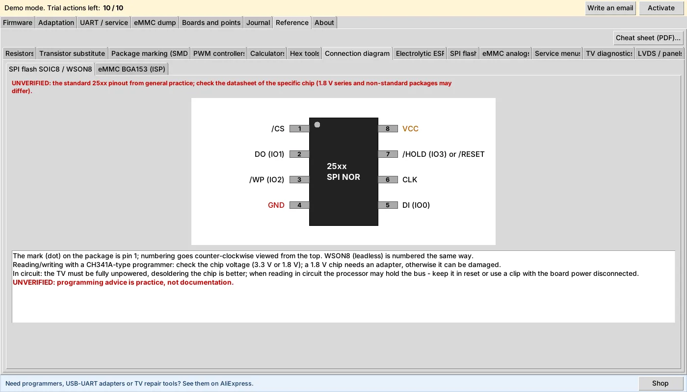
| Pin | Signal |
|---|---|
| 1 | /CS |
| 2 | DO (IO1) |
| 3 | /WP (IO2) |
| 4 | GND |
| 5 | DI (IO0) |
| 6 | CLK |
| 7 | /HOLD (IO3) or /RESET |
| 8 | VCC |
The mark (dot) on the package is pin 1; numbering goes counter-clockwise viewed from the top. The leadless WSON8 is numbered the same way.
Voltage: 3.3 V or 1.8 V
Before connecting a CH341A-type programmer, check the chip supply voltage. A 1.8 V chip needs an adapter, otherwise it can be damaged.
In-circuit and off-board reading
- It is better to desolder the chip: this removes the influence of other devices on the bus.
- If you read in circuit, the TV must be fully unpowered. The processor may hold the bus, so keep it in reset or use a clip with the board power disconnected.
These recommendations are practice, not documentation.
Choosing a chip
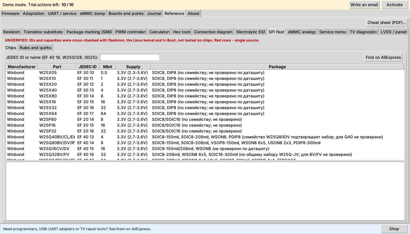
The FW Tool reference has an SPI flash table searchable by JEDEC ID or name: manufacturer, size in Mbit, supply, packages. Rows confirmed by a single source are marked red.